<More to be added here>
Graphics Shifting Modes
When the Alphanumeric
Mode Disable field is set to 1, the sequencer operates in graphics
mode where data in memory references pixel values, as opposed to the character
map based operation used for alphanumeric mode.
The sequencer has three
methods of taking the 32-bit memory location loaded and shifting it into
4-bit pixel values suitable for graphics modes, one of which combines 2
pixel values to form 8-bit pixel values. The first method is the
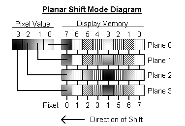
one used for the VGA's 16 color modes. This mode is selected when
both the 256-Color Shift Mode and Shift
Register Interleave Mode fields are set to 0. In this mode, one
bit from each of the four 8-bit planes in the 32-bit memory is used to
form a 16 color value. This is shown in the diagram below, where the most
significant bit of each of the four planes is shifted out into a pixel
value, which is then sent to the attribute controller to be converted into
an index into the DAC palette. Following this, the remaining bits
will be shifted out one bit at a time, from most to least significant bit,
with the bits from planes 0-3 going to pixel bits 0-3.
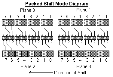
The second shift mode is
the packed shift mode, which is selected when both the 256-Color
Shift Mode field is set to 0 and the Shift
Register Interleave Mode field is set to 1.This is used by the VGA
bios to support video modes compatible with CGA video modes. However,
the CGA only uses planes 0 and 1 providing for a 4 color packed mode; however,
the VGA hardware actually uses bits from two different bit planes, providing
for 16 color modes. The bits for the first four pixels shifted out
for a given address are stored in planes 0 and 2. The second four
are stored in planes 1 and 3. For each pixel, bits 3-2 are shifted
out of the higher numbered plane and bits 1-0 are shifted out of the lower
numbered plane. For example, bits 3-2 of the first pixel shifted
out are located in bits 7-6 of plane 2; likewise, bits 1-0 of the same
pixel are located in bits 7-6 of plane 0.
The third shift mode is used for
256-color modes, which is selected when the 256-Color
Shift Mode field is set to 1 (this field takes precedence over the
Shift Register Interleave Mode field.)
This behavior of this shift mode varies among VGA implementations, due
to it normally being used in combination with the 8-bit
Color Enable field of the attribute controller. Thus certain
variances in the sequencing operations can be masked by similar variances
in the attribute controller. However, the implementations I have
experimented with seem to fall into one of two similar behaviors, and thus
it is possible to describe both here. Note that one is essentially
a mirror image of the other, leading me to believe that the designers knew
how it should work to be 100% IBM VGA compatible, but managed to get it
backwards in the actual implementation. Due to being very poorly documented
and understood, it is very possible that there are other implementations
that vary significantly from these two cases. I do, however, feel
that attempting to specify each field's function as accurately possible
can allow more powerful utilization of the hardware.
When this shift mode is
enabled, the VGA hardware shifts 4 bit pixel values out of the 32-bit memory
location each dot clock. This 4-bit value is processed by the attribute
controller, and the lower 4 bits of the resulting DAC index is combined
with the lower 4 bits of the previous attribute lookup to produce an 8-bit
index into the DAC palette. This is why, for example, a 320 pixel
wide 256 color mode needs to be programmed with timing values for a 640
pixel wide normal mode. In 256-color mode, each plane holds a 8-bit
value which is intended to be the DAC palette index for that pixel.
Every second 8-bit index generated should correspond to the values in planes
0-3, appearing left to right on the display. This is masked by the
attribute controller, which in 256 color mode latches every second 8-bit
value as well. This means that the intermediate 8-bit values are
not normally seen, and is where implementations can vary. Another
variance is whether the even or odd pixel values generated are the intended
data bytes. This also is masked by the attribute controller, which
latches the appropriate even or odd pixel values.
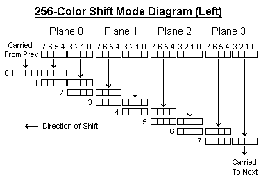
The first case is where
the 8-bit values are formed by shifting the 4 8-bit planes left.
This is shown in the diagram below. The first pixel value generated
will be the value held in bits 7-4 of plane 0, which is then followed by
bits 3-0 of plane 0. This continues, shifting out the upper four
bits of each plane in sequence before the lower four bits, ending up with
bits 3-0 of plane 3. Each pixel value is fed to the attribute controller,
where a lookup operation is performed using the attribute table.
The previous 8-bit DAC index is shifted left by four, moving from the lower
four bits to the upper four bits of the DAC index, and the lower 4 bits
of the attribute table entry for the current pixel is shifted into the
lower 4 bits of the 8-bit value, producing a new 8-bit DAC index.
Note how one 4-bit result carries over into the next display memory location
sequenced.
For example, assume planes
0-3 hold 01h, 23h, 45h, and 67h respectively, and the lower 4 bits of the
the attribute table entries hold the value of the index itself, essentially
using the index value as the result, and the last 8-bit DAC index generated
was FEh. The first cycle, the pixel value generated is 0h, which is fed
to the attribute controller and looked up, producing the table entry 0h
(surprise!) The previous DAC index, FEh, is shifted left by four bits,
while the new value, 0h is shifted into the lower four bits. Thus,
the new DAC index output for this pixel is E0h. The next pixel is
1h, which produces 1h at the other end of the attribute controller.
The previous DAC index, E0h is shifted again producing 01h. This
process continues, producing the DAC indexes, in order, 12h, 23h, 34h,
45h, 56h, and 67h. Note that every second DAC index is the appropriate
8-bit value for a 256-color mode, while the values in between contain four
bits of the previous and four bits of the next DAC index.
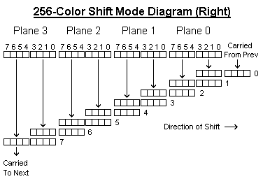
The second case is where the 8-bit
values are formed by shifting the 8-bit values right, as depicted in the
diagram below. The first pixel value generated is the lower four
bits of plane 0, followed by the upper four bits. This continues
for planes 1-3 until the last pixel value produced, which is the upper
four bits of Plane 3. These pixel values are fed to the attribute
controller, where the corresponding entry in the attribute table is looked
up. The previous 8-bit DAC index is shifted right 4 places. and the
lower four bits of the attribute table entry generated is used as the upper
four bits of the new DAC index.
For example, assume planes
0-3 hold 01h, 23h, 45h, and 67h respectively, and the lower 4 bits of the
the attribute table entries hold the value of the index itself, essentially
using the index value as the result, and the last 8-bit DAC index generated
was FEh. The first cycle, the pixel value generated is 1h, which is fed
to the attribute controller and looked up, producing the table entry 1h.
The previous DAC index, FEh, is shifted right by four bits, while the new
value, 1h is shifted into the upper four bits. Thus, the new DAC
index output for this pixel is 1Fh. The next pixel is 0h, which produces
0h at the other end of the attribute controller. The previous DAC
index, 1Fh is shifted again producing 01h. This process continues,
producing the DAC indexes, in order, 30h, 23h, 52h, 45h, 74h, and 67h.
Again, note that every second DAC index is the appropriate 8-bit value
for a 256-color mode, while the values in between contain four bits of
the previous and four bits of the next DAC index.
Notice: All trademarks used or referred to on this page are the property
of their respective owners.
All pages are Copyright © 1997, 1998, J. D. Neal, except where
noted. Permission for utilization and distribution is subject to the terms
of the FreeVGA Project Copyright License.